Researchers Develop Nano-antennas for Ultra-Fast Wireless Connections
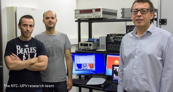
A group of researchers have designed new silicon nano-antennas with direct applications in communications and data processing for the next generation reconfigurable photonic chips. This type of configuration opens the door to the development of new miniature nano-biosensors and to the design of future systems and networks based on quantum optics. The research group belongs to the Nanophotonic Technology Centre (NTC) of the Polytechnic University of Valencia (UPV).
The results of the research conducted by the NTC-UPV team combine the benefits of dielectric wireless applications and the benefits of plasmonics. This opens the path to a new generation of ultra-integrated hybrid networks, which is the main contribution of the research. According to Javier Martí, head of the Nanophotonic Technology Centre of the UPV, the team experimentally proved the first wireless dielectric-plasmonic connection thanks to a new type of dielectric nanoantenna that overcomes the limitations of plasmonics, opening the door to new hybrid configurations.
The results obtained have a direct implication in the design of reconfigurable communication networks inside the chip, in the development of ultra-fast optic devices, and in the practical implementation of ultra-compact biosensors. Thanks to plasmonic structures, this also opens the door to the creation of interfaces with future quantum systems.
According to Sergio Lechago, a researcher at the NTC and co-author of the study, the plasmonic devices have enabled the development of important applications in fields such as spectroscopy, near-field and sensing optic microscopy, thanks to their unique capability of manipulating light on a nano level. Within the communications integrated in the chip, plasmonics enable the development of ultra-compact and affordable devices (modulators, detectors or sources) that can function at very high operation speeds with low energy consumption.
According to Sergio’s fellow co-author of the study from the NTC, Carlos García Meca, the natural way of interconnecting these devices in the optic chip is by using metallic nanoguides. However, guiding light through these devices leads to very high propagation losses and entails certain restrictions regarding reconfigurability.
The use of plasmonic nanoantennas has been proposed to replace and improve the performance of guided metallic interconnections, but these antennas have low directivity and high losses which hinder their use in many practical applications. In this work, we overcame all these limitations by introducing a new dielectric nanoantenna design that acts as an efficient interface for plasmonic systems. This makes it possible to combine the benefits of plasmonics with those of silicon photonics, which can lead to more efficient, fast and reconfigurable chips.
This new breakthrough developed in the laboratories of the Centre of Nanophotonic Technology of the UPV could also be applied to fields such as biochemical or agri-food industries, thanks to the role that these hybrid systems can carry out as sensors with multiple purposes, allowing the interaction of light with nanoscopic organic and inorganic structures.
The work of the UPV researchers has been published in the ACS Photonics journal.

